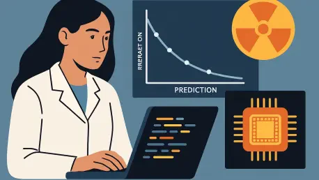

Imagine a satellite orbiting Earth for decades, its delicate electronic heart exposed to relentless cosmic radiation, silently degrading with each passing day until a critical failure jeopardizes an entire mission. This scenario isn’t just a thought experiment—it’s a pressing reality for industries like space exploration and medical imaging, where chips must endure extreme conditions. Radiation damage in semiconductors poses a significant threat, especially as technology shrinks to ever-smaller scales, making components more vulnerable. Enter a groundbreaking solution from the world of open-source technology: a design kit that models how chips age under radiation stress. Developed by a research team at Fraunhofer IIS, this tool offers a transparent way to predict and mitigate damage, promising to revolutionize how engineers approach reliability in high-stakes environments. This innovation isn’t just about keeping circuits alive—it’s about democratizing access to vital design resources for a wider range of creators.
Unlocking the Power of Open-Source Design Kits
At the heart of this technological leap is an open process design kit (PDK) that stands as a game-changer for engineers grappling with radiation effects. Unlike traditional proprietary models guarded by chip vendors, this open-source framework lays bare detailed data on how transistors and other circuit elements behave under long-term radiation exposure. It empowers designers to simulate degradation over extended periods, such as a 10-year span, using lab-tested parameters and mathematical predictions to pinpoint potential failure points. This level of insight allows for smarter planning—integrating protective measures early without bloating power use or chip size. Moreover, the transparency of the tool breaks down barriers that smaller companies, startups, and academic labs often face when excluded from vendor data. By offering a clear window into component limits, it fosters innovation in fields where reliability is non-negotiable, like satellites hovering in orbit or CT scanners enduring high-energy X-rays. The shift to open access signals a broader trend: complex engineering challenges can be tackled collaboratively, leveling the playing field.
Bridging Gaps in High-Radiation Environments
Looking ahead, the implications of this open-source approach extend far beyond technical specs, reshaping how industries prepare for harsher operational realities. As chips continue to miniaturize, their susceptibility to radiation-induced faults—whether silent wear or sudden crashes—grows exponentially, posing risks in critical applications. This tool not only addresses that vulnerability but also builds a bridge for diverse innovators to design resilient electronics for extreme settings, from deep-space missions to advanced medical systems. Its publicly available models and simulations enable a wider community to test and refine circuits, ensuring they withstand punishing conditions over time. Furthermore, this initiative reflected a growing consensus that accessible radiation modeling is essential for next-generation hardware. By empowering smaller players to compete in high-stakes arenas, it sparked fresh ideas and solutions that proprietary systems often stifle. Looking back, this step was a turning point, proving that collaborative tools could drive reliability and inclusivity hand in hand, setting a precedent for future challenges.