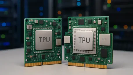

The global demand for computational power has reached a critical inflection point where the sheer scale of artificial intelligence models is testing the physical boundaries of semiconductor engineering and energy sustainability. At the Google Cloud Next conference, a landmark shift in hardware strategy was unveiled with the introduction of the eighth-generation Tensor Processing Unit (TPU) refresh. For the first time since the TPU’s debut a decade ago, the company has abandoned its traditional one-size-fits-all hardware approach, choosing instead to split its silicon ecosystem into two specialized processors: the TPU 8t and the TPU 8i. This development marks a calculated effort to overcome the “memory wall”—the physical bottleneck where data transfer speeds fail to keep pace with raw computational power—by providing hardware specifically tuned for different phases of the AI lifecycle.
This strategic pivot is more than a simple performance upgrade; it is a fundamental realignment of how cloud infrastructure serves the needs of massive-scale generative models. By offering a dual-track hardware path, Google aims to provide the foundational infrastructure necessary for the next generation of trillion-parameter models and real-time autonomous agents. This move recognizes that the computational requirements for training a model are fundamentally different from those required to serve that model to millions of users simultaneously. Consequently, the eighth generation represents a sophisticated attempt to optimize the economic and physical efficiency of the modern data center, ensuring that intelligence remains both scalable and cost-effective.
Historical Context and the Shift Toward Hardware Specialization
The journey toward the TPU 8 series is rooted in over a decade of internal innovation designed to reduce dependency on general-purpose hardware. Since the mid-2010s, the industry has relied heavily on Graphics Processing Units (GPUs) for AI tasks, but as models grew into the trillions of parameters, the limitations of general-purpose silicon became an unavoidable obstacle. Historically, Google’s TPU program focused on a singular, versatile chip; however, the rising complexity of “mixture of experts” (MoE) models and the demand for real-time AI agents necessitated a more granular approach. This eighth-generation release reflects a broader industry shift where “intelligence per watt” and “intelligence per dollar” have replaced raw clock speed as the primary metrics of success in the cloud-compute landscape.
As the industry moved from simple neural networks to transformer-based architectures, the bottleneck shifted from pure arithmetic logic to the ability to move data across massive clusters. This historical context is vital because it explains why a single chip design is no longer sufficient to maintain a competitive edge. By the start of the current decade, it became clear that a training-focused chip was often over-engineered for simple inference tasks, leading to wasted power and capital. Conversely, chips optimized for low-latency response lacked the massive memory bandwidth required to ingest the vast datasets used during the training phase. The TPU 8 series addresses these historical inefficiencies by embracing specialization as a core design principle.
Optimizing Training and Inference Through Specialized Architecture
Engineering the TPU 8t for Massive-Scale Training Efficiency
The TPU 8t is a powerhouse designed specifically for the rigorous demands of training the world’s largest AI models, where consistent throughput is the most critical metric. Operating at an unprecedented scale, individual “pods” of TPU 8t chips can contain up to 9,600 units, offering a twofold increase in memory bandwidth and a fourfold increase in networking bandwidth over the previous generation. This design allows researchers to push the boundaries of model size without being throttled by the speed at which data can be fed into the processor. However, the true innovation lies in the introduction of “goodput”—a measure of consistent, productive compute time that accounts for the inevitable hardware failures that occur at such a massive scale.
With 2 petabytes of shared high-bandwidth memory and a self-healing architecture that can reroute data around faulty links, the TPU 8t targets a 97% goodput rate. This ensures that training cycles for massive language models continue uninterrupted, even when individual hardware components fail, which is a common occurrence in clusters containing thousands of interconnects. By automating the recovery process and minimizing downtime, Google has created a system where the “cost of failure” is significantly reduced. This reliability is essential for enterprises that cannot afford to lose weeks of training progress due to a single faulty cable or memory module, making the TPU 8t the gold standard for high-stakes model development.
Overcoming the Memory Wall with the TPU 8i
While training requires throughput, inference requires speed and low latency to ensure that AI applications feel responsive to human users. The TPU 8i is optimized for this latter stage, where trained models must respond to queries in real-time without the perceptible lag that often plagues large-scale deployments. The 8i utilizes a custom Inter-Chip Interconnect (ICI) layer known as “Boardfly,” which doubles memory bandwidth while physically shortening the distance between chips. This architectural pivot is vital for modern AI agents that rely on dynamic model activation, where only specific parts of a model are used to answer a given question.
By reducing the time it takes to retrieve data from memory, the TPU 8i effectively bridges the “memory wall,” allowing for the seamless, instantaneous interactions required by the next wave of generative AI applications. This specialization means that the 8i can handle more queries per second than a general-purpose chip while consuming less power. For businesses deploying AI at scale, this translates to lower operational costs and a better user experience. The ability to serve complex models with minimal latency ensures that AI can be integrated into consumer-facing products, such as real-time translation and interactive customer service agents, without compromising on performance.
Navigating the Rivalry: ASICs and General-Purpose GPUs
The launch of the TPU 8 series intensifies the competition between Google’s Application-Specific Integrated Circuits (ASICs) and Nvidia’s general-purpose GPUs. While Nvidia’s ecosystem offers unmatched flexibility and a “scale-up” philosophy that appeals to a wide variety of workloads, Google’s “single machine philosophy” allows its chips to function as a unified entity within a global address space. This integrated approach eliminates the latency overhead often found in traditional data center networking protocols like InfiniBand. Furthermore, by focusing on specialized silicon, Google can offer higher energy efficiency, which has become a primary concern for data center operators facing strict power constraints.
As the industry matures, the choice between these two philosophies becomes a matter of strategic alignment. Nvidia remains the leader for those who require versatility and broad software compatibility across different cloud providers. In contrast, Google’s TPU ecosystem offers a highly optimized, vertically integrated stack that provides superior performance for those willing to commit to the Google Cloud environment. This rivalry is driving rapid innovation, as both companies race to solve the cooling and power delivery challenges associated with increasingly dense compute clusters. Ultimately, the market is shifting toward a landscape where the specific architecture of the chip is just as important as the software running on it.
Emerging Trends and the Future of AI Factories
The release of the TPU 8t and 8i points toward a future defined by “AI factories” rather than simple data centers. A key trend shaping this evolution is the resurgence of the Central Processing Unit (CPU) as a necessary partner to specialized AI silicon. Google’s Axion custom Arm CPUs are designed to work alongside TPUs, handling general-purpose tasks like code execution, data preprocessing, and result verification. Expert predictions suggest that the “age of specialization” is just beginning; as general-purpose performance gains slow down, we can expect to see even more specialized chips dedicated to specific sub-tasks within the AI ecosystem.
This move toward heterogeneous compute—combining CPUs, training chips, and inference chips—will likely become the standard for all major cloud providers seeking to maximize their return on investment. The concept of the AI factory implies a shift in thinking, where every component of the data center, from the power grid to the liquid cooling systems, is tuned for the specific purpose of generating intelligence. This industrialization of AI requires not only better chips but also more sophisticated management software that can orchestrate workloads across thousands of specialized processors. As these factories become more efficient, the cost of generating a single “token” of AI output will continue to drop, making the technology accessible to a broader range of industries and applications.
Actionable Insights for the AI-Driven Enterprise
For businesses and developers, the arrival of the TPU 8 series offers several strategic takeaways that should inform their infrastructure investments. First, the bifurcation of hardware means that organizations can now choose infrastructure that is cost-optimized for their specific needs—whether they are building a model from scratch or deploying one for millions of users. Best practices now suggest moving away from “brute force” compute and toward architectures that prioritize reliability and energy efficiency. To maximize ROI, companies should look for cloud environments that offer a tight integration between specialized AI chips and high-performance CPUs to handle the complex logic that surrounds modern AI models.
Applying these insights means evaluating AI providers not just on the number of chips they offer, but on the sophistication of their interconnects and the overall resilience of their hardware stack. Organizations should prioritize “goodput” over theoretical peak performance, as the ability to maintain a consistent training schedule is often more valuable than raw speed. Furthermore, as energy costs and environmental regulations become more stringent, selecting energy-efficient ASIC architectures can provide a significant long-term competitive advantage. By aligning their technical strategy with the trend of hardware specialization, enterprises can ensure that their AI initiatives remain both sustainable and scalable in an increasingly crowded market.
Conclusion: A New Standard for Cloud Intelligence
Google’s eighth-generation TPU refresh represented more than a simple hardware iteration; it functioned as a fundamental redesign of the infrastructure required to sustain the AI boom. By launching the TPU 8t and 8i, the company successfully addressed the physical limits of memory and networking while embracing the necessity of specialized silicon. This move ensured that as AI models became more complex and the demand for real-time agents grew, the underlying hardware supported them reliably and sustainably. The introduction of technologies like the Boardfly interconnect and the focus on “goodput” provided a new framework for measuring the effectiveness of cloud compute, shifting the focus from raw power to operational resilience.
The strategic shift toward specialized processors established a clear path for the future of technological infrastructure. It moved the industry away from a reliance on general-purpose hardware and toward a more efficient, heterogeneous model of computing. By integrating custom CPUs with specialized AI accelerators, the eighth generation of TPUs cemented the transition from traditional data centers to high-efficiency AI factories. Ultimately, this launch set a high bar for the global technology landscape, proving that the next phase of digital transformation would be defined by the ability to manage complexity at an unprecedented scale while maintaining the economic and environmental efficiency required for long-term growth.